http://english.cas.cn/newsroom/research_news/phys/202502/t20250214_901725.shtml
https://www.nature.com/articles/s41586-025-08711-x
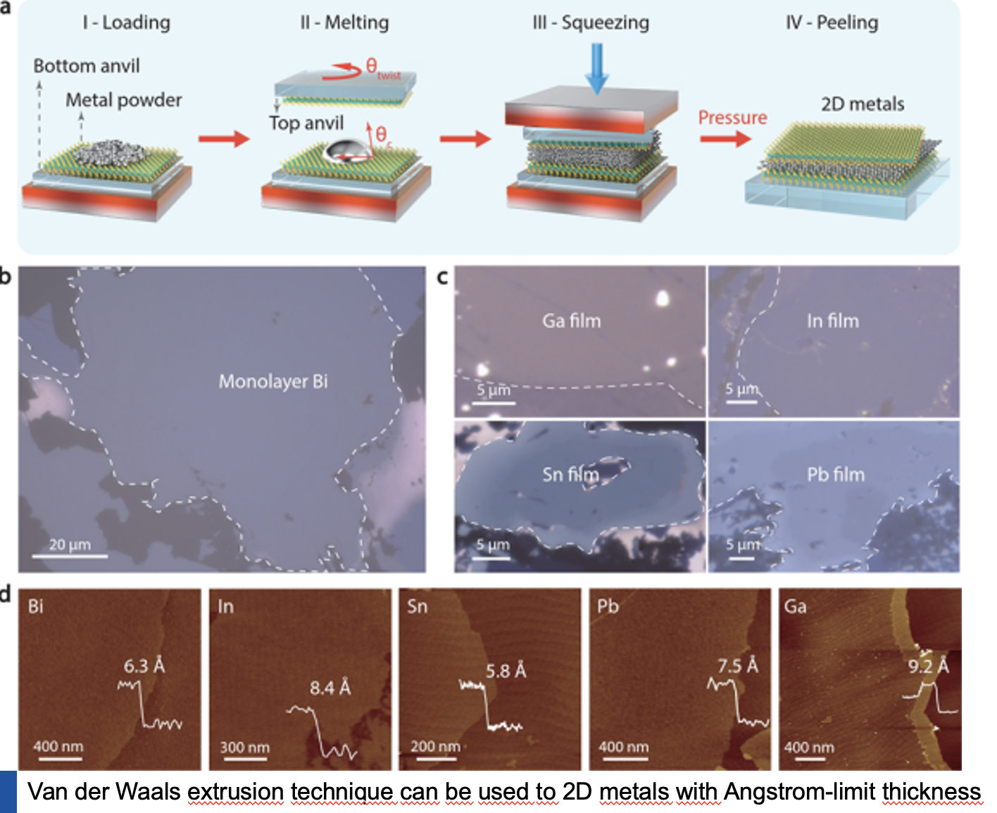
Researchers from the CAS Institute of Physics (IOP) have developed a convenient, universal, atomic-level manufacturing technique—called vdW squeezing—for the production of 2D metals at the Angstrom thickness limit. The manufacturing technique involves melting and squeezing pure metals between two rigid vdW anvils under high pressure. With this method, the researchers produced diverse atomically thin 2D metals, including Bi (~6.3 Å), Sn (~5.8 Å), Pb (~7.5 Å), In (~8.4 Å) and Ga (~9.2 Å).
The vdW anvils consist of two single-crystalline MoS2 monolayers epitaxially grown on sapphire. The anvils are essential for producing 2D metals for two reasons. First, the atomically flat, dangling-bond-free surface of the monolayer MoS2/sapphire ensures uniform 2D metal thickness over a large scale. Second, the high Young’s modulus of both sapphire and monolayer MoS2 (> 300 GPa) allows them to withstand extreme pressures, enabling 2D metals formed between the two anvils to approach their angstrom thickness limit.
The 2D metals synthesized via this process were stabilized through complete encapsulation between two MoS2 monolayers, making them environmentally stable and ensuring non-bonded interfaces. This structure facilitated device fabrication by allowing access to their intrinsic transport properties, which were previously unavailable. Electrical and spectroscopic measurements of monolayer Bi revealed excellent physical properties, including significantly enhanced electrical conductivity, a strong field effect with p-type behavior, large nonlinear Hall conductivity, and new phonon modes.